|
AFBR-S50 API Reference Manual v1.6.6
AFBR-S50 Time-of-Flight Sensor SDK for Embedded Software
|
|
AFBR-S50 API Reference Manual v1.6.6
AFBR-S50 Time-of-Flight Sensor SDK for Embedded Software
|
The following section gives an brief overview on how to integrate the AFBR-S50 Core Library and API into an user application and how to port the library to another platform. See the Fig. 4.1 for a visualization of the integration progress. The API is embedded into the user application where both are accessing the hardware peripherals via the driver and HAL layers.
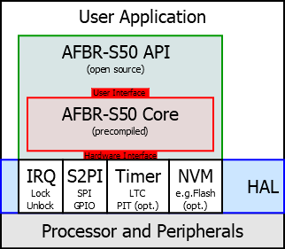
The basic idea to port the API to a new platform is to adjust the HAL to the new hardware and implement the functionality that is required by the core library to interface with the AFBR-S50 sensor device through the given peripherals. The following sections give an overview on the hardware interface layers and finally show a step-by-step guide on how to accomplish the porting task.
The AFBR-S50 Core Library is build and tested using the GNU Embedded Toolchain for Arm. However, any other toolchain that supports AEABI compatible library linking should work fine with the library files. Note that builds that utilize these toolchains are not tested nor verified and can not be officially supported!
If you still have to use one of these, make sure to read the Binary Interoperability Between Toolchains Application Note by ARM to understand the implications of mixing code from different toolchains.
As mentioned above, the AFBR-S50 Core Library is build with AEABI compatibility enabled (i.e. with the -library_interface=aeabi_clib compiler flag). The following GNU toolchain settings are used to compile the libraries:
-library_interface=aeabi_clib: Specifies that the compiler output is AEABI compliant.-mfloat-abi=softfp: Software floating-point Procedure Call Standard (PCS) and hardware floating point instructions.wchar_t values at all.The AFBR-S50 Core Library is compatible with all Arm Cortex-M Series Processors. The library is optimized for the smallest variants, the Cortex-M0/M0+. However, the upwards compatibility of the Cortex-Mx family makes it easy to run the same library on higher architectures without effort as well. The library artifacts are compiled for the most common architectures.
The following API variants are available:
| Library Name | Architecture | FPU | ABI | Optimization |
|---|---|---|---|---|
afbrs50_m0 | Cortex-M0/M0+ | none | soft | performance |
afbrs50_m0_os | Cortex-M0/M0+ | none | soft | memory size |
afbrs50_m3 | Cortex-M3 | none | soft | performance |
afbrs50_m3_os | Cortex-M3 | none | soft | memory size |
afbrs50_m4 | Cortex-M4/M7 | none | soft | performance |
afbrs50_m4_os | Cortex-M4/M7 | none | soft | memory size |
afbrs50_m4_fpu | Cortex-M4/M7 | FPv4-SP | hard | performance |
afbrs50_m4_fpu_os | Cortex-M4/M7 | FPv4-SP | hard | memory size |
Architecture:
-mcpu=cortex-m0-mcpu=cortex-m3-mcpu=cortex-m4FPU (Fixed-Point Unit)
none: No floating-point hardware unitFPv4-SP: Hardware floating-point support (-mfpu=fpv4-sp-d16)ABI (Application Binary Interface):
-mfloat-abi=soft)-mfloat-abi=hard)Optimization Level:
-O3)-Os)-mfloat-abi=softfp GNU compiler flag, enabling the software floating-point PCS and hardware floating-point instruction support. The AFBR-S50 Core Library and API does not use any floating point operations anyhow.The AFBR-S50 Core Library is build and tested using the NXP FRDM-KL46Z development platform that contains a ARM Cortex-M0+ processor. The instruction set available on the Cortex-M0 is a subset of all the instruction sets available on higher Cortex-Mx processor cores like ARM Cortex-M3 or ARM Cortex-M4. Therefore the library can be used on any Cortex-Mx based platforms that contain the required hardware peripherals. These are:
Mandatory hardware peripherals are
Furthermore, optional peripherals are
Minimum memory requirements:
The following section gives a brief overview on the corresponding hardware layers.
The AFBR-S50 API basically supports any ARM Cortex-Mx based microcontroller platform. Merely the hardware layers need to be adopted to match the underlying hardware. The API defines interfaces for all required hardware modules and the corresponding methods. Refer Fig. 4.1 to get an overview of the required hardware abstraction layer modules. The interfaces are assembled in the platform module of the API. Each module contains a detailed description on how to implement the corresponding interface. The enclosed example code that comes with the AFBR-S50 SDK also provides implementations of the hardware layers based on the NXP MKL46z platform as a reference. See the getting started section on how to build and run the examples on the provided evaluation platform.
The AFBR-S50 core has the capability to perform the device operation self-sustained in the background by hopping from interrupt to interrupt without blocking the main processor thread. Therefore all peripheral drivers must be implemented asynchronously, such that an operation is invoked from the API and returns immediately. After finishing the corresponding operation, a callback must be invoked in order to perform the next step in the current sequence. Especially, for the timer interface, there is the requirement of periodic interrupts to be invoked in order to start the measurement cycle in the background without the requirement to call the corresponding function from the application main thread. However, in order to not overload the processor (i.e. from within the interrupt service routines), the data evaluation must be executed from the main thread after the raw measurement data has been read from the device.
The S2PI module is a combination of SPI and GPIO hardware. The communication with the device requires an SPI peripheral. To increase speed and lower the CPU load, it is recommended to use a DMA module along with the SPI interface. The measurement data ready event occurs when the measurement cycle on the device is finished and the data is ready to read. A single GPIO IRQ invoking a callback to the API core is required and incorporated into the SPI module.
In addition to the standard SPI interface, the corresponding pins must also be accessible in GPIO mode. This is required to access the EEPROM memory of the AFBR-S50 sensor device that holds calibration parameters. The EEPROM interface is connected to the SPI pins to decrease the complexity in pinning and wiring. The EEPROM interface is not compatible with any standard SPI interface and thus it is emulated in software using bit banging algorithms. A mechanism to switch forth and back between SPI and GPIO mode for the corresponding pins is incorporated into the S2PI module.
The module needs to provide two different modes of operation, both as SPI master:
A fast SPI mode for accessing the device
The fast SPI mode is used for accessing the device for all purposes (initialization, configuration, calibration and measurement).
Obviously, to allow a continuous data transfer on the SPI interface without creating a high load on the microcontroller itself, although not strictly required, it is strongly recommended to set up DMA transfer for the SPI interface. The following description assumes that DMA is used.
A slow GPIO mode for accessing the EEPROM
Calibration data is stored on a small EEPROM that needs to be read upon device initialization at a much lower speed. The readout is performed on the same interface as the fast SPI, but with a bit-banging mechanism that allows the control of all signals with a much slower timing as GPIOs.
The bit-banging mechanism is already built into the library, so the hardware layer only has to provide:
The EEPROM readout is performed only during initialization, so the speed does not negatively affect measurement performance.
See the S2PI module documentation for more details on the SPI interface.
The SPI hardware layer is required to be initialized before the first call to the core library.
CLK, MOSI, MISO
The SPI communications requires the three standard pins CLK (SPI clock), MOSI (master out, slave in) and MISO (master in, slave out) to be switchable between SPI and GPIO modes.
The CLK and MOSI lines are configured as output and the MISO is configured as input. The MISO is actively driven by the device and thus no pull-up resistor is required.
CS
Even though it is expected that the device is the only device on the SPI interface, a CS (chip select) signal is required to be asserted on every SPI transfer. Depending on the SPI capabilities, this may be either handled by the SPI peripheral (hard CS) or by GPIO toggling (soft CS).
This signal is active low and is asserted during transfers. The signal must be cycled to high between transfers.
IRQ
This is an input line that allows the device to signal that measurement data is available and ready for transfer.
This signal is active low and will be asserted until the next SPI transfer is started, which is assumed to pick up the data. The GPIO should be configured as input triggering an interrupt on the falling edge. Take care that a GPIO with a unique interrupt ID is picked for this line, or no other GPIO attached to the same interrupt ID is configured to trigger any interrupts. The IRQ line needs a pull-up resistor set.
Be also careful with the initialization regarding:
The following table provides an overview over the GPIO configurations:
| CLK | MOSI | MISO | CS | IRQ | |
|---|---|---|---|---|---|
| Direction | Output | Output | Input | Output | Input |
| Drive Mode | Push-Pull | Push-Pull | - | Push-Pull | - |
| Pull-Up | - | - | None | - | Pull Up |
| Interrupt | - | - | - | - | Falling Edge |
| Speed | Fast | Fast | Fast | Fast | Fast |
| Signal Level | 3V3 | 3V3 | 3V3 | 3V3 | 3V3 |
| Mode for SPI | SPI | SPI | SPI | SPI or GPIO | GPIO |
| Mode for GPIO | GPIO | GPIO | GPIO | GPIO | (not used) |
The device works with CPOL=1 (clock polarity) and CPHA=1 (clock phase), meaning that the clock is pulled high in idle state and the data should be read on the rising clock edge. This is also frequently referred to SPI mode 3. This must be configured accordingly:
CPOL = 1CPHA = 1The speed is crucial to achieve a high frame rate when performing continuous measurements: As each measurement requires around 500 bytes of data, the data transfer alone will take 4000 times the SPI clock period, not including the measurement itself and the preparation of the SPI transfers.
It is therefore recommended to choose a high transfer speed that is still compatible with the electrical requirements of the sensor as given in the data sheet and the environment in which it is built. An SPI clock frequency in the range of 10 to 12 MHz is a good starting point.
For the DMA (direct memory access) transfer, usually two separate channels need to be set up for the data read and write.
As the kind of operation always has to be specified by the master within the transfer, the SPI transfers have only two modes:
Both kinds of transfer are started via the S2PI_TransferFrame() function. While the txData pointer always points to valid data, the rxData pointer is set to 0 if no data shall be transmitted.
rxData and txData frequently point to the same memory address. While this should usually be no problem, as the memory byte needs to be read before and stored after the transmission, make sure that the DMA implementation of your MCU supports this! Otherwise, the received data should be transferred to a temporary buffer and copied to the destination after reception.Usually, the SPI transmission requires a callback function to be triggered after the transmission is complete.
Typically, in the DMA setup, the device provides DMA complete interrupts that can call the callback function. Also, if the CS signal is applied as GPIO (soft CS), it can be unasserted here.
However, this DMA complete callback function may already start the next SPI transfer immediately. So all cleanups required after the current SPI transfer needs to be performed before that. This may be complicated as two DMA channels may be involved in the transmit and receive case and perform cleanup on their individual channel only. The callback function must be triggered only after both channels are freed and cleaned up. Also, the CS must be unasserted before the callback function is called.
On the other hand, in the transmit only case, make sure that the DMA interrupt does not call the callback function, or unassert CS, before the last byte is fully transmitted, especially if the SPI speed is slow.
To make use of stable and high frame rates, the SPI interrupt should not be blocked by other possibly longer running interrupts, so the interrupt priority should be chosen sufficiently high. On the other hand, if the target application uses other interrupts for very time sensitive purposes, they should have higher priority, as the callback function may include preparing a new SPI transfer and therefore may take multiple microseconds to return.
An important thing to note is that the API will trigger new SPI transfers within the SPI and GPIO callback functions.
The Timer Interface implements two timers: a lifetime counter (LTC) for time measurement duties and a periodic interrupt timer (PIT) for the triggering of measurements on a time based schedule.
The lifetime counter should be set up to deliver the current time in microseconds. The timer resolution must be in the magnitude of 10 to 100 microseconds. This means, however, that the systick counter driven by the systick interrupt cannot be used, as it typically provides an accuracy in the range of milliseconds.
Basically a hardware and a software approach can be chosen to implement the lifetime counter functionality. In any case, a first timer with at least 16-bit width is set to count the sub-seconds value and the prescaler is preferably set such that the timer wraps around after exactly 1 second. In case of a 16-bit counter the maximum achievable granularity is approximately 15 (1/65336) microseconds which is suitable for most applications.
In a hardware based scenario, a second timer with 32-bits is chained to increase its value whenever the first counter wraps around and thus counting seconds. In a software based scenario, the first timer triggers an interrupt upon the wrap around. A 32-bit software counter representing the seconds is increased within the interrupt service routine.
Note that the periodic interrupt timer is mandatory only if the user requires the measurements to be started autonomously in the background on a time based schedule. Simple implementations may trigger measurements on demand from the foreground thread and thus the PIT is not required. A weak implementation is provided within the library so that it is not required to implement the interface if the PIT is not used.
A different timer than the timer for the lifetime counter should be used. Usually, the maximum period that will be used can be reached by a combination of the timer reload value and the prescaler even on a 16-bit timer. Extending the period with software is also possible. This can be done by using an additional software counter that counts up every time the interrupts occurs and invokes the callback only after a given number has been reached.
The granularity of the PIT is highly dependent on the required measurement frame rate. E.g. to achieve 1000 frames per seconds, the PIT must be able to trigger every millisecond!
As described in the sections about the S2PI and Timer layers, the Argus API uses three different kinds of interrupts associated with callback functions that have to be set up during the module initialization:
All of these interrupts with their callbacks typically take several microseconds to complete. The callback functions within the API are designed to not induce considerable delays and return as fast as possible.
If other interrupts within the microcontroller are used, their priority should be chosen in the following way:
The callbacks from the interrupts above provide information or trigger new SPI transfers. In order to prevent concurrency issues, the program must be able to lock the occurrence of these interrupts in atomic or critical sections of the code. Therefore, the IRQ Interface shall be implemented.
In general, the IRQs are only locked for very short time (sub-microseconds) in order read the status and update it appropriately without the interruption from a higher priority thread. However a nested implementation of the locking mechanism is required for the library core to work correctly.
Refer to the module documentation to see an example implementation that locks all maskable interrupts. If other critical interrupts are present, an alternative implementation can selectively lock only the interrupts used by the Argus API.
The Non-Volatile Memory (NVM) layer is an optional interface that provides access to a non-volatile memory hardware, e.g. flash. This is used to permanently save calibration parameters that can be gained by executing the corresponding calibration sequences from the [Calibration module](Calibration). Also user set calibration parameters can be saved into the NVM in order to be available after a system reset or power cycle. If custom calibration parameters does not need to be save within the API, the implementation of the interface can be skipped. A weak implementation is provided in the core library that will disable the NVM feature.
In order to send debug and error messages, a printf-like function from the Debug Interface can be implemented. If not required, the implementation can be left out and and dummy default implementation will be used that does not send the error messages anywhere. However, implementing this interface may have an impact on the measurement performance, especially when it is slow (e. g. synchronous transfer over UART).
Note that errors are propagated using the status_t enumeration of status and error codes. Any method within the API returns an error code that gives a hint on the execution status of the routine.
The HAL Self Test module is provide to help the user to verify its ported code on the new platform. It runs a series of simple tests on the target platform and verifies things like SPI, GPIO and timer implementations. In case of timer tests, the connected AFBR-S50 sensor device is used as a reference clock in order to verify the correct timings. Please refer to the HAL Self Test module for a detailed documentations.
Here is the modified Advanced Example from the Getting Started section. The changes are basically an additional include directive and the call to the Argus_VerifyHALImplementation function. The function call is placed after hardware initialization (i.e. hardware_init) and before device initialization (i.e. Argus_Init).
Please find the example files in [INSTALL_DIR]\Device\Examples\ (default is C:\Program Files (x86)\Broadcom\AFBR-S50 SDK\Device\Examples\).
The HAL self test header and source files are located under [INSTALL_DIR]\Device\Examples\test\ (default is C:\Program Files (x86)\Broadcom\AFBR-S50 SDK\Device\Examples\test\).
01_simple_example_with_hal_self_test.c 02_advanced_example_with_hal_self_test.c
The following step-by-step guide leads through the basic process on getting the API running on any Cortex-M0 based development environment. The steps are demonstrated using the MCUXpresso-IDE and the NXP FRDM-KL46Z development platform from NXP that comes also with the AFBR-S50 evaluation kit. It should be an easy task for experienced embedded software developer to follow the steps on its dedicated development environment.
The first step would be to create a new empty project or use an existing one. Usually this is done utilizing the provided platform specific SDK provided by the vendor. In case of the FRDM-KL46Z, the MCUXpresso-IDE and the MCUXpresso-SDK is used to create a project with at least SPI (with DMA mode), GPIO and PIT (periodic interrupt timer) support. The new project is tested using the "Hello World" print statement.
After the successfully creating, building and testing the new SDK project, the hardware interfaces required by the AFBR-S50 Core Library need to implemented. Basically there are two approaches: either forward the commands to the provided SDK functionality from the MCU vendor or implement an individual version from scratch.
In order to start, the include files must be referenced in the project and a source file is required for each interface file. The simplest way to include the API into your project is to copy the files. Go to the install directory if the AFBR-S50 SDK and find the files in [INSTALL_DIR]\Device\Lib (see Fig. 4.3).
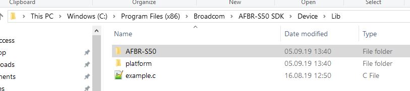
The AFBR-S50 library and include files are in the AFBR-S50 folder which needs to be copied into the project.
Note: The example.c file as well as the platform folder belonging to the examples. See the Getting Started Guide for more information. The platform contains reference implementation of the platform layer which can also be referred for customers implementations.
The include path to the AFBR-S50 header (AFBR-S50\Include) files must be added to the project setting. Afterwards and source file for each individual header file in the AFBR-S50\Include\platform folder must be created and filled with definitions for each function declaration in the header files. Therefore the following files are created:
argus_s2pi.cargus_log.cargus_timer.cargus_irq.c .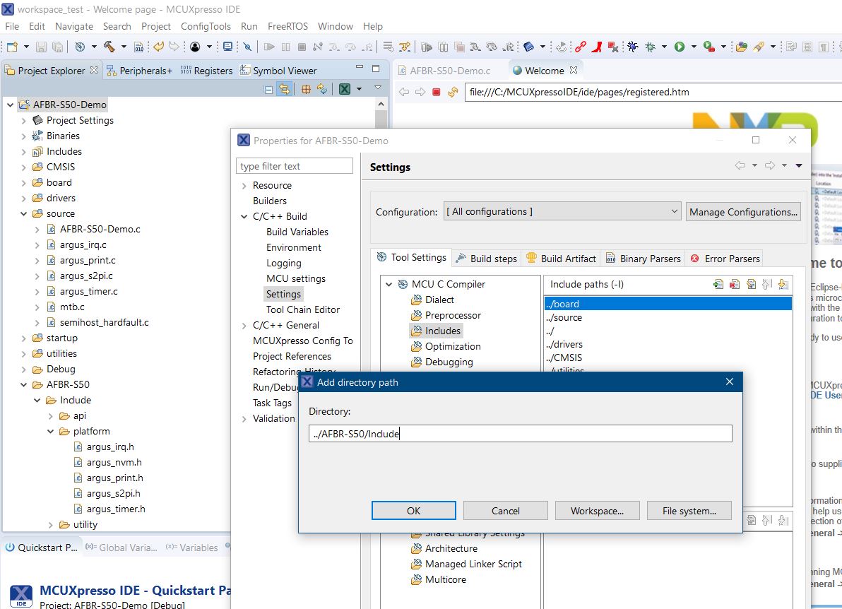
Note that the argus_nvm.h is ignored in this examples since the usage of the NVM is not required for this demonstration. Default implementations in the AFBR-S50 library core will be used that do not use any non-volatile memory module.
For example, the argus_timer.c file could look like this with empty function bodies:
After testing the build, implement the actual function bodies. Don't forget to implement and call initialization code as well if required.
Here is a simple example of a timer function:
Please refer to the platform interface module documentation on details on how to correctly implement the individual layer. Also refer the example implementations of the platform layers that come with the AFBR-S50 SDK, found in [INSTALL_DIR]\Device\Lib\platform\driver. These are:
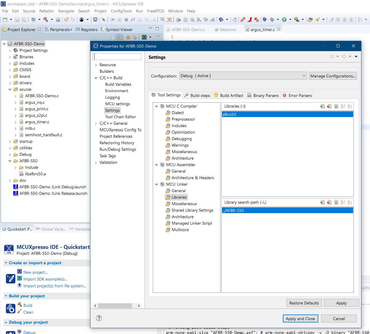
irq.c: implements a basic version of the interrupt locking mechanism that allows nested locking which is declared in argus_irq.h.s2pi.c: implements the combined SPI and GPIO interface declared in argus_s2pi.h.timer.c: implements the timer functionality declared in argus_timer.h.uart.c: contains the function definition for the [argus_log.h](Debug: Logging Interface) header and implements a print functionality over an UART interface. .Now that the platform layers are implemented, the library needs to be linked into the project. Therefore add the AFBR-S50 folder ([INSTALL_DIR]\\Device\\Lib\\AFBR-S50) to the library search path and the libafbrs50.a file to the linker libraries (i.e. afbrs50, leaving away the lib and .a in case of GNU toolchain).
Now, the AFBR-S50 API is ready to use. Include the argus.h header and start coding your AFBR-S50 application. Refer to the Getting Started Guide to see an example implementation with basic measurements.